
Mosfet de potência smd 110v STC2326
obtenha o ultimo preço| Tipo de pagamento: | L/C,T/T,Paypal |
| Incoterm: | FOB,CFR,CIF |
| transporte: | Ocean,Air |
| porta: | SHANGHAI |

| Tipo de pagamento: | L/C,T/T,Paypal |
| Incoterm: | FOB,CFR,CIF |
| transporte: | Ocean,Air |
| porta: | SHANGHAI |
Modelo: YZPST-STC2326
marca: YZPST
B triacs da série TA30
YZPST-STC2326
DESCRIÇÃO
O STC2326 é o transistor de efeito de campo de potência do modo de aprimoramento lógico de canal N, que é produzido usando tecnologia de trincheira DMOS de densidade celular super alta. O STC2326 foi projetado especificamente para melhorar a eficiência geral dos conversores DC / DC usando controladores PWM de comutação síncronos ou convencionais. Ele foi otimizado para baixa carga de gate, RDS baixo (ON) e velocidade de comutação rápida.
APLICAÇÕES
Sistema alimentado
Conversor DC / DC
Interruptor de carga
CARACTERÍSTICAS
110V / 3A, RDS (ON) = 310mΩ @ VGS = 10V
Design de célula de alta densidade para RDS extremamente baixo (ON)
Excepcional resistência à corrente e capacidade máxima de corrente contínua
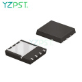
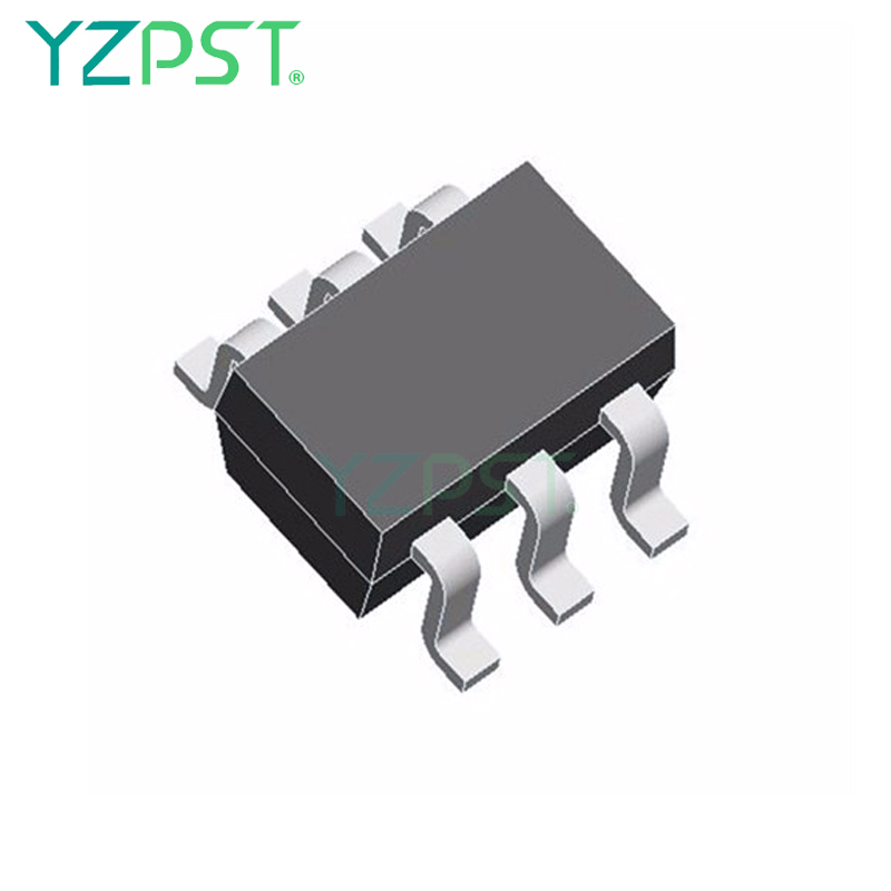
Design de embalagem SOT-23-6L
CONFIGURAÇÃO DO PINO (SOT-23-6L)
")
|
Pin |
Symbol |
Description |
|
1 |
D |
Drain |
|
2 |
D |
Drain |
|
3 |
G |
Gate |
|
4 |
S |
Source |
|
5 |
D |
Drain |
|
6 |
D |
Drain |
O RING ING EM F O R M A T I O N
|
Part Number |
Package |
Part Marking |
|
SPN2326S26RGB |
SOT-23-6L |
26YW |
A B SOU L T E MA X I M U M R A T IN G S ( T A = 25 ℃ U n l e s s O U T r i s e w N O T d e)
|
Parameter |
Symbol |
Typical |
Unit |
|
|
Drain-Source Voltage |
VDSS |
110 |
V |
|
|
Gate –Source Voltage |
VGSS |
±20 |
V |
|
|
Continuous Drain Current(TJ=150℃) |
TA=25℃ |
ID |
3.0 |
A |
|
TA=70℃ |
2.0 |
|||
|
Pulsed Drain Current |
IDM |
10 |
A |
|
|
Power Dissipation |
TA=25℃ |
PD |
2.0 |
W |
|
TA=70℃ |
1.3 |
|||
|
Operating Junction Temperature |
TJ |
-55/150 |
℃ |
|
|
Storage Temperature Range |
TSTG |
-55/150 |
℃ |
|
|
Thermal Resistance-Junction to Ambient |
RθJA |
62.5 |
℃/W |
|
|
Parameter |
Symbol |
Conditions |
Min. |
Typ |
Max. |
Unit |
|
Static |
||||||
|
Drain-Source Breakdown Voltage |
V(BR)DSS |
VGS=0V,ID=250uA |
110 |
|
|
V |
|
Gate Threshold Voltage |
VGS(th) |
VDS=VGS,ID=250uA |
1 |
2.0 |
2.5 |
|
|
Gate Leakage Current |
IGSS |
VDS=0V,VGS=±20V |
|
|
±100 |
nA |
|
Zero Gate Voltage Drain Current |
IDSS |
VDS=80V,VGS=0V |
|
|
1 |
uA |
|
VDS=80V,VGS=0V TJ=125℃ |
|
|
5 |
|||
|
On-State Drain Current |
ID(on) |
VDS≥5V,VGS =10V |
3.0 |
|
|
A |
|
Drain-Source On-Resistance |
RDS(on) |
VGS= 10V,ID=3A |
|
0.26 |
0.31 |
Ω |
|
Forward Transconductance |
gfs |
VDS=10V,ID=3A |
|
2.4 |
|
S |
|
Diode Forward Voltage |
VSD |
IS=1A,VGS =0V |
|
|
1.2 |
V |
|
Dynamic |
||||||
|
Total Gate Charge |
Qg |
VDS=80V,VGS=10V ID= 5A |
|
9 |
13 |
nC |
|
Gate-Source Charge |
Qgs |
|
2 |
|
||
|
Gate-Drain Charge |
Qgd |
|
1.4 |
|
||
|
Input Capacitance |
Ciss |
VDS=25,VGS=0V f=1MHz |
|
508 |
|
pF |
|
Output Capacitance |
Coss |
|
29 |
|
||
|
Reverse Transfer Capacitance |
Crss |
|
16.5 |
|
||
|
Turn-On Time |
td(on) |
VDD=50V,RL=10Ω ID=3A,VGEN=10V RG=3.3Ω |
|
2 |
|
nS |
|
tr |
|
21.5 |
|
|||
|
Turn-Off Time |
td(off) |
|
11.2 |
|
||
|
tf |
|
18.8 |
|
|||
")
")


Número De Telefone: 86-514-87782298
Whatsapp: +8613805278321
Endereço: 3rd Floor, Weiheng Building No.20 B Area, Yangzhou, Jiangsu China
site: https://pt.yzpst.com


Privacy statement: Your privacy is very important to Us. Our company promises not to disclose your personal information to any external company with out your explicit permission.
Fill in more information so that we can get in touch with you faster
Privacy statement: Your privacy is very important to Us. Our company promises not to disclose your personal information to any external company with out your explicit permission.