
Controle de fase 25TTS12 semicondutores scr 1200V
$0.252000-99999 Piece/Pieces
$0.22≥100000Piece/Pieces
| Tipo de pagamento: | L/C,T/T,Paypal |
| Incoterm: | FOB,CFR,CIF |
| Quantidade de pedido mínimo: | 2000 Piece/Pieces |
| transporte: | Ocean,Air |
| porta: | SHANGHAI |

$0.252000-99999 Piece/Pieces
$0.22≥100000Piece/Pieces
| Tipo de pagamento: | L/C,T/T,Paypal |
| Incoterm: | FOB,CFR,CIF |
| Quantidade de pedido mínimo: | 2000 Piece/Pieces |
| transporte: | Ocean,Air |
| porta: | SHANGHAI |
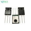
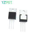
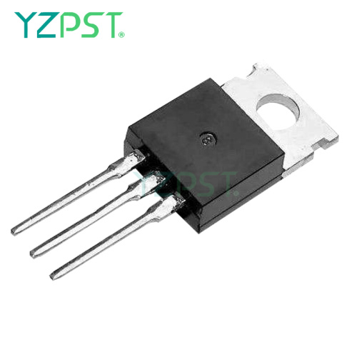
Modelo: YZPST-25TTS12-1
marca: YZPST
| Unidades de venda | : | Piece/Pieces |
| Tipo de pacote | : | 1. Embalagem anti-eletrostática 2. Caixa de papelão 3. Embalagem protetora de plástico |
Controle de fase SCR, 25 A
DESCRIÇÃO / CARACTERÍSTICAS
A série de alta tensão 25TTS de retificadores controlados por silício é projetada especificamente para aplicações de comutação de potência média e controle de fase. A tecnologia de passivação de vidro usada tem operação confiável até
Temperatura de junção de 125 ° C.
As aplicações típicas estão na retificação de entrada (partida suave) e esses produtos são projetados para serem usados com diodos de entrada, interruptores e retificadores de saída Vishay HPP, que estão disponíveis em contornos de pacote idênticos.
Este produto foi projetado e qualificado para o nível industrial.

|
PRODUCT SUMMARY |
|
|
VT at 16 A |
< 1.25 V |
|
ITSM |
300 A |
|
VRRM |
800/1200 V |
|
OUTPUT CURRENT IN TYPICAL APPLICATIONS |
|||
|
APPLICATIONS |
SINGLE-PHASE BRIDGE |
THREE-PHASE BRIDGE |
UNITS |
|
Capacitive input filter TA = 55 °C, TJ = 125 °C, common heatsink of 1 °C/W |
18 |
22 |
A |
|
MAJOR RATINGS AND CHARACTERISTICS |
|||
|
PARAMETER |
TEST CONDITIONS |
VALUES |
UNITS |
|
IT(AV) |
Sinusoidal waveform |
16 |
A |
|
IRMS |
|
25 |
|
|
VRRM/VDRM |
|
800/1200 |
V |
|
ITSM |
|
300 |
A |
|
VT |
16 A, TJ = 25 °C |
1.25 |
V |
|
dV/dt |
|
500 |
V/µs |
|
dI/dt |
|
150 |
A/µs |
|
TJ |
|
- 40 to 125 |
°C |
|
VOLTAGE RATINGS |
|||
|
PART NUMBER |
VRRM, MAXIMUM PEAK REVERSE VOLTAGE V |
VDRM, MAXIMUM PEAK DIRECT VOLTAGE V |
IRRM/IDRM AT 125 °C mA |
|
25TTS08 |
800 |
800 |
10 |
|
25TTS12 |
1200 |
1200 |
|
|
ABSOLUTE MAXIMUM RATINGS |
||||||
|
PARAMETER |
SYMBOL |
TEST CONDITIONS |
VALUES |
UNITS |
||
|
TYP. |
MAX. |
|||||
|
Maximum average on-state current |
IT(AV) |
TC = 93 °C, 180° conduction half sine wave |
16 |
A |
||
|
Maximum RMS on-state current |
IRMS |
|
25 |
|||
|
Maximum peak, one-cycle, non-repetitive surge current |
ITSM |
10 ms sine pulse, rated VRRM applied |
300 |
|||
|
10 ms sine pulse, no voltage reapplied |
350 |
|||||
|
Maximum I2t for fusing |
I2t |
10 ms sine pulse, rated VRRM applied |
450 |
A2s |
||
|
10 ms sine pulse, no voltage reapplied |
630 |
|||||
|
Maximum I2√t for fusing |
I2√t |
t = 0.1 to 10 ms, no voltage reapplied |
6300 |
A2√s |
||
|
Maximum on-state voltage drop |
VTM |
16 A, TJ = 25 °C |
1.25 |
V |
||
|
On-state slope resistance |
rt |
TJ = 125 °C |
12.0 |
mΩ |
||
|
Threshold voltage |
VT(TO) |
1.0 |
V |
|||
|
Maximum reverse and direct leakage current |
IRM/IDM |
TJ = 25 °C |
VR = Rated VRRM/VDRM |
0.5 |
mA |
|
|
TJ = 125 °C |
10 |
|||||
|
Holding current |
IH |
Anode supply = 6 V, resistive load, initial IT = 1 A |
- |
100 |
||
|
Maximum latching current |
IL |
Anode supply = 6 V, resistive load |
200 |
|||
|
Maximum rate of rise of off-state voltage |
dV/dt |
|
500 |
V/µs |
||
|
Maximum rate of rise of turned-on current |
dI/dt |
|
150 |
A/µs |
||
|
TRIGGERING |
||||
|
PARAMETER |
SYMBOL |
TEST CONDITIONS |
VALUES |
UNITS |
|
Maximum peak gate power |
PGM |
|
8.0 |
W |
|
Maximum average gate power |
PG(AV) |
|
2.0 |
|
|
Maximum peak positive gate current |
+ IGM |
|
1.5 |
A |
|
Maximum peak negative gate voltage |
- VGM |
|
10 |
V |
|
Maximum required DC gate current to trigger |
IGT |
Anode supply = 6 V, resistive load, TJ = - 10 °C |
60 |
mA |
|
Anode supply = 6 V, resistive load, TJ = 25 °C |
45 |
|||
|
Anode supply = 6 V, resistive load, TJ = 125 °C |
20 |
|||
|
Maximum required DC gate voltage to trigger |
VGT |
Anode supply = 6 V, resistive load, TJ = - 10 °C |
2.5 |
V |
|
Anode supply = 6 V, resistive load, TJ = 25 °C |
2.0 |
|||
|
Anode supply = 6 V, resistive load, TJ = 125 °C |
1.0 |
|||
|
Maximum DC gate voltage not to trigger |
VGD |
TJ = 125 °C, VDRM = Rated value |
0.25 |
|
|
Maximum DC gate current not to trigger |
IGD |
2.0 |
mA |
|
|
SWITCHING |
||||
|
PARAMETER |
SYMBOL |
TEST CONDITIONS |
VALUES |
UNITS |
|
Typical turn-on time |
tgt |
TJ = 25 °C |
0.9 |
µs |
|
Typical reverse recovery time |
trr |
TJ = 125 °C |
4 |
|
|
Typical turn-off time |
tq |
110 |
||
|
THERMAL AND MECHANICAL SPECIFICATIONS |
|||||
|
PARAMETER |
SYMBOL |
TEST CONDITIONS |
VALUES |
UNITS |
|
|
Maximum junction and storage temperature range |
TJ, TStg |
|
- 40 to 125 |
°C |
|
|
Maximum thermal resistance, junction to case |
RthJC |
DC operation |
1.1 |
°C/W |
|
|
Maximum thermal resistance, junction to ambient |
RthJA |
|
62 |
||
|
Typical thermal resistance, case to heatsink |
RthCS |
Mounting surface, smooth and greased |
0.5 |
||
|
Approximate weight |
|
|
2 |
g |
|
|
0.07 |
oz. |
||||
|
Mounting torque |
minimum |
|
|
6 (5) |
kgf · cm (lbf · in) |
|
maximum |
|
|
12 (10) |
||
|
Marking device |
|
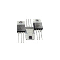
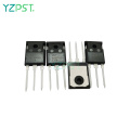
Case style TO-220AB |
25TTS08 |
||
|
25TTS12 |
|||||


Número De Telefone: 86-514-87782298
Whatsapp: +8613805278321
Endereço: 3rd Floor, Weiheng Building No.20 B Area, Yangzhou, Jiangsu China
site: https://pt.yzpst.com


Privacy statement: Your privacy is very important to Us. Our company promises not to disclose your personal information to any external company with out your explicit permission.
Fill in more information so that we can get in touch with you faster
Privacy statement: Your privacy is very important to Us. Our company promises not to disclose your personal information to any external company with out your explicit permission.