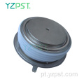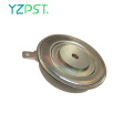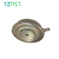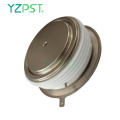
Tiristor promocional de alta potência para controle de fase
obtenha o ultimo preço| Tipo de pagamento: | L/C,T/T,Paypal |
| Incoterm: | FOB,CFR,CIF |
| transporte: | Ocean,Air |
| porta: | Shanghai |

| Tipo de pagamento: | L/C,T/T,Paypal |
| Incoterm: | FOB,CFR,CIF |
| transporte: | Ocean,Air |
| porta: | Shanghai |
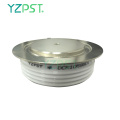
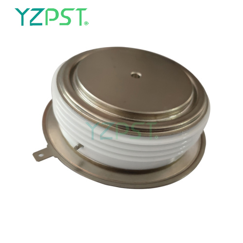
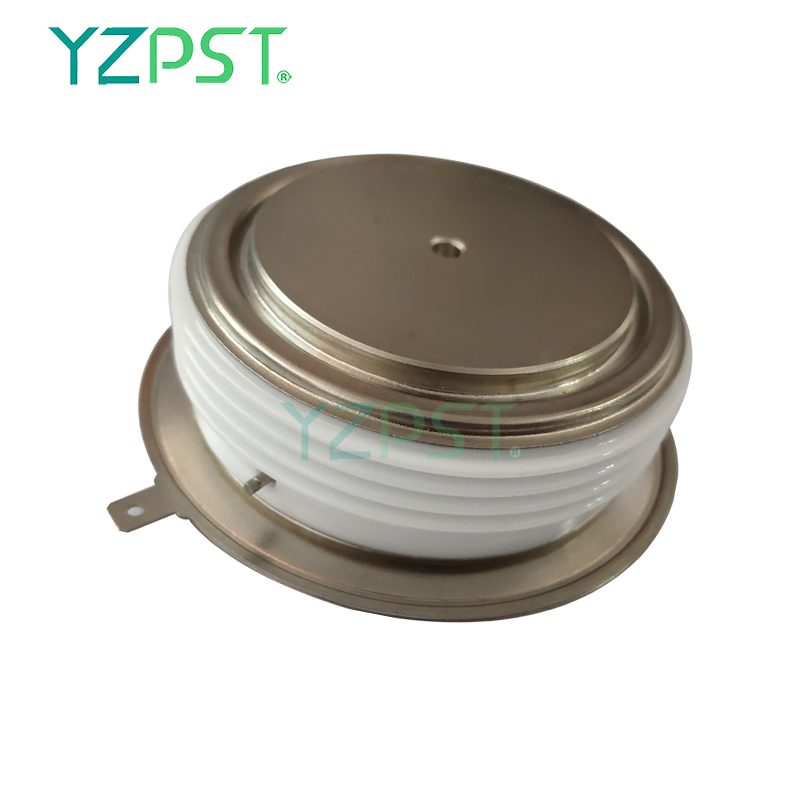
Modelo: YZPST-R219CH12FN0
marca: YZPST
Tiristor de alta potência para controle de fase
YZPST-R219CH12FN0
Recursos:
.Tempo máximo de desligamento garantido
. Toda a estrutura difusa
. Dispositivo montado sob pressão
Configuração da porta de amplificação interdigitada
. Alta capacidade dV / dt
CARACTERÍSTICAS ELÉTRICAS E CLASSIFICAÇÕES
Estado de bloqueio - desativado
|
|
|
VRRM (1) |
VDRM (1) |
VRSM (1) |
|
1200 |
1200 |
1300 |
V RRM = tensão reversa de pico repetitiva
V DRM = Tensão de estado de pico repetitivo
V RSM = Tensão reversa de pico não repetitiva (2)
|
Repetitive peak reverse leakage and off state leakage |
IRRM / IDRM |
15 mA 70 mA (3) |
|
Critical rate of voltage rise |
dV/dt (4) |
200 V/msec |
Notas:
Todas as classificações são especificadas para Tj = 25 o C, salvo indicação em contrário.
(1) Todas as classificações de tensão são especificadas para um
Forma de onda senoidal de 50Hz / 60zHz sobre o
faixa de temperatura -40 a +125 o C.
(2) 10 ms. máx. largura do pulso
(3) Valor máximo para Tj = 125 o C.
(4) Valor mínimo para forma de onda linear e exponencial até 80% V DRM nominal. Portão aberto. Tj = 125 o C.
(5) Valor não repetitivo.
(6) O valor de di / dt é estabelecido de acordo com com o padrão EIA / NIMA RS-397, seção 5-2-2-6. O valor definido seria, além de que a obtida a partir de um circuito ubber, compreendendo um 0,2 m M condensador e 20 ohmsresistance em paralelo com o thristor sob teste.
Condução - no estado
|
Parameter |
Symbol |
Min. |
Max. |
Typ. |
Units |
Conditions |
|
Max. average value of on-state current |
IT(AV)M |
|
929 |
|
A |
Sinewave,180o conduction,Tc=55oC |
|
RMS value of on-state current |
IT(RMS)m |
|
1893 |
|
A |
Nominal value |
|
Peak one cPSTCle surge (non repetitive) current |
ITSM |
|
-
9.0 |
|
kA
kA |
8.3 msec (60Hz), sinusoidal wave- shape, 180o conduction, Tj = 125 oC 10.0 msec (50Hz), sinusoidal wave- shape, 180o conduction, Tj = 125 oC |
|
I square t |
I2t |
|
405x103 |
|
A2s |
8.3 msec |
|
Latching current |
IL |
|
- |
|
mA |
VD = 24 V; RL= 12 ohms |
|
Holding current |
IH |
|
1000 |
|
mA |
VD = 24 V; I = 2.5 A |
|
Peak on-state voltage |
VTM |
|
2.04 |
|
V |
ITM = 1400 A |
|
Critical rate of rise of on-state current (5, 6) |
di/dt |
|
1500 |
|
A/ms |
Switching from VDRM £ 1000 V, non-repetitive |
|
Critical rate of rise of on-state current (6) |
di/dt |
|
1000 |
|
A/ms |
Switching from VDRM £ 1000 V |
Gating
|
Parameter |
Symbol |
Min. |
Max. |
Typ. |
Units |
Conditions |
|
Peak gate power dissipation |
PGM |
|
30 |
|
W |
|
|
Average gate power dissipation |
PG(AV) |
|
2 |
|
W |
|
|
Peak gate current |
IGM |
|
- |
|
A |
|
|
Gate current required to trigger all units |
IGT |
|
300 |
|
mA |
VD = 10 V;IT=3A;Tj = +25 oC
|
|
Gate voltage required to trigger all units
|
VGT |
|
3.0 |
|
V
|
VD = 10 V;IT=3A;Tj = +25 oC
|
|
Peak negative voltage |
VRGM |
|
5 |
|
V |
|
Dinâmico
|
Parameter |
Symbol |
Min. |
Max. |
Typ. |
Units |
Conditions |
|
Delay time |
tgd |
|
1.0 |
- |
ms |
VD=67% VDRM, IT=2000A, di/dt=60A/us, IFG=2A, tr=0.5us, Tj=25C |
|
Turn-on time |
tgt |
|
2.0 |
- |
|
|
|
Turn-off time (with VR = -5 V) |
tq |
- |
- |
10 |
ms |
ITM=1000A, tp=1000us, di/dt=60A/us, Vr=50V, Vdr=33%VDRM, dVdr/dt=200V/us |
|
Reverse recovery current |
Irm |
|
- |
|
A |
ITM=4000A, tp=2000us, di/dt=60A/us |


Número De Telefone: 86-514-87782298
Whatsapp: +8613805278321
Endereço: 3rd Floor, Weiheng Building No.20 B Area, Yangzhou, Jiangsu China
site: https://pt.yzpst.com


Privacy statement: Your privacy is very important to Us. Our company promises not to disclose your personal information to any external company with out your explicit permission.
Fill in more information so that we can get in touch with you faster
Privacy statement: Your privacy is very important to Us. Our company promises not to disclose your personal information to any external company with out your explicit permission.